 |
| About Bioline | All Journals | Testimonials | Membership | News |
|
||||||
|
||||||
Journal of Applied Sciences & Environmental Management, Vol. 9, No. 1, 2005, pp. 143-145 Studies on a-Se/n-Si and a-Te/n-Si Heterojunctions *S.E. IYAYI1; A. A. OBERAFO2 1Department of Physics, AmbroseAlliUniversity, P.M.B.
14, Ekpoma, Edo State, Nigeria. Email: sunnyiyayi@yahoo.com Code Number: ja05026 ABSTRACT: Heterojunctions are fabricated by depositing amorphous selenium (a-Se) and amorphous tellurium (a-Te) films on n-type single (n-Si) wafers by the method of vacuum evaporation. The silicon wafers have surface orientation of (111). Resistivity of each silicon wafer is 5Ω-cm and carrier concentration of 8.30 x 1014cm-3. Two of the junction devices are annealed in a vacuum for half an hour. Current-voltage measurements are made at room temperature (298K). Rectification properties are observed in all the junctions. Barrier heights of a-Se/n-Si junctions are higher than a-Te/n-Si junctions. The current density in annealed junctions is lower than in as-deposited (unannealed) counterpart. @JASEM
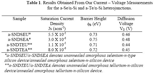
Heterojuncton devices have also been studied from the viewpoint of understanding fundamental device physics. Such studies include band structure, current transport mechanism and as tools in the analysis of other physical parameters. For example, Sinha and Misra, 1983 studied the current-voltage characteristics of the junction between amorphous germanium and monocrystal p-Si at different temperatures. The authors found that the junction exhibits almost ideal Schottky diode behaviour in a narrow region of applied bias. However, the junction current at large external bias (V>300mV) is dominated by tunneling. Amorphous Selenium (aSe) and amorphous tellurium (aTe) may be obtained by thermal evaporation of materials in a vacuum. According to Kazmerski, 1980 amorphous thin films posses a large density of dangling bonds, which defy doping attempts because dopants attach themselves to these bonds. The purpose of this study is to measure the electrical properties of thermally evaporated amorphous selenium and tellurium films on n-type crystalline silicon substrates and assess the junctions for possible device application. MATERIALS AND METHODS Four highly polished n-type (111) – oriented silicon wafers each of 5Ω-cm resistivity, carrier concentration of 8.30 x 1014cm-3 and 17.50mm in diameter are first cleaned with soap and distilled water and blow dried in a jet of nitrogen gas. The silicon wafers are further cleaned in trichloroethylene vapour. Etching is done in a 2:1:1 parts by volume in CP6 solution, 2HNO3 (50%), 1HF (25%) and 1CH2COOH (25%) for 3 minutes followed by rinsing in distilled water. The selenium and tellurium films are deposited on the silicon substrates at room temperature (298K) with a resistivity heated molybdenum boat in a vacuum of about 10-5 torr (1.33mPa). The junctions are circular in shape with approximate area of 0.28cm2. The thickness of each deposited thin film is 1000Å as determined by Edward Film Thickness Monitor, model FTM3. Four samples are fabricated together. Two of the junctions are annealed in a vacuum chamber at a temperature of 420K for 30 minutes. The annealed junctions are allowed to cool slowly to obtain equilibrium structures. Antimony (Sb) electrodes are deposited on the a-Se and a-Te side with a device area of 0.13cm2 while Indium-mercury (InHg) forms the back contact on the crystalline silicon substrates, after first cleaning the silicon surface with diamond paste and acetone. The current-voltage measurements are performed at room temperature (298K) in an evacuated cryostat. RESULTS AND DISCUSSION The results for the room temperature current density-voltage (J-V) characteristics of all fabricated junctions are shown in Table 1. For forward bias such that VF >3KBT/q, the forward current-voltage characteristic for a junction diode is described by the thermionic emission relation, where KB is the Botzman's constant, q is the electronic charge, T is the absolute temperature and n is the ideality factor (diode quality factor) defined as According to Okumura and Tu, 1987 the ideality factor n is unity when the current flow across the diode is by thermionic emission, and it increases with the degradation of the diode characteristics or with other superimposing transport mechanism. The constant, JS is the saturation current density (forward current density at zero bias), which provided n = 1, is usually assumed to be the value given by thermionic emission theory, where A** is the effective Richardson constant modified to take account of both the effective mass of the electrons in the semiconductor and the results of the thermionic emission-diffusion synthesis. The constant, JS is obtained by the extrapolation of the linear region of lnJF versus VF curve to zero bias. From equation (3), the barrier height, φB is obtained as,
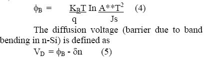
where δn, the distance in energy from Fermi level to conduction band is determined to be 0.27V. An analysis of the forward- and reverse biased current-voltage characteristics of the junctions show rectification properties. For forward voltages, VF < 1.0V, the forward characteristics shows exponential behaviour, the current increasing rapidly with voltage according to equation (1). As the bias is increased further, deviation from this exponential behaviour sets in with the current increasing less and less rapidly than exp (qVF/nKBT). Kuech et al, 1984attributes such a drop in exponential rate of increase of forward current with increasing bias to the influence of an appreciable series resistance on the junction characteristics. Krupanidhi et al, 1983 also found a similar behaviour in As2Te3-nSi heterojunctions. In the reverse direction, the current increases with voltage exhibiting a rather weak saturation up to about 10V. We observe from Table 1 that a-Te/n-Si junctions have higher current densities than a-Se/n-Si junctions. This can be explained on the basis of the density of electronic states in both selenium and tellurium. Tellurium has a large density of states at the Fermi level, which reveals the more "metallic" behaviour in this material. These large densities of states make it reasonable that they contribute more significantly to the electrical conduction in a-Te/n-Si. Thus barrier heights of a-Se/n-Si junctions are found to be higher than that of a-Te/n-Si junctions in accordance with equation (4). Further analysis of the current-voltage characteristics of the junctions show that the room electrical conductivity is decreased after post-deposition heat treatment (annealing). As shown in Table 1, the current densities of the annealed junctions are lower than that for the as-deposited (unannealed) junctions. The localized states at the interface of the junction and the high density of localized states in the bulk of amorphous layer contribute significantly to the electrical conductivity. In fact, the dominant current mechanism in the amorphous layer of the junction is essentially by hopping between the localized states. However, annealing reduces the number of these states and therefore the conductivity. Table 1 shows that the barrier height is generally sensitive to heat treatment; there is an increase in barrier height after annealing. The reduction of density of localized states by annealing leads to reduction in current density and hence an increase in barrier heights. Read et al, 1994 found a similar behaviour in Si3N4/Si/Ge interface where the interface trap states decreased by a factor of 5 after thermal annealing. Conclusion: The room temperature (298K) current-voltage characteristics of a-Se/n-Si and a-Te/n-Si heterojunctions are studied. The heterojunctions show rectification properties, hence can be used as rectifying devices in electronic appliances. The electrical conductivity in the junctions decrease with annealing. Barrier heights of a-Se/n-Si junctions are found to be higher than in a-Te/n-Si junctions. Acknowledgements: We would like to thank Dr A.A. Oberafo for providing the silicon wafers and the evaporated materials (Se and Te) for fabricating the devices. REFERENCES
Copyright 2005 - Journal of Applied Sciences & Environmental Management
The following images related to this document are available:Photo images[ja05026t1.jpg] |
| |||||||||
